Custom thumbnail...
Introduction
Hello it's a me Drifter Programming! Today we get back to Logic Design and VHDL to get into the promised "advanced" implementation of a specific mathematical operation in Hardware! First things first "you should know VHDL programming" and so I suggest you to read my VHDL series that you can find in the last Recap if you haven't already and if you don't know VHDL already (of course!). The system that we will implement will also contain RAM and ROM modules/components and so the two explanation and implementation posts about that should also be in your watch-list.
Today's post will be about:
- explaining the problem
- analyzing it
- creating a software model (c-code)
- setting up an architecture that can solve it in hardware
So, without further do, let's get started!
The mathematical problem
We want to implement the following modulo 2 multiplication:

which can else be written as:

And so we have:
- A line-matrix A[M] of M-elements
- A mxn matrix H[M][N] of MxN-elements
- A result line-matrix R[N] of N-elements
Note that the amount of columns of A must be equal to the amount of rows of H, cause else the multiplication can't be done (Linear Algebra)
But, what do I mean with modulo 2? Modulo 2 means that:
- All the elements of the matrices are 1-bit in length
- Each multiplication is equal to a boolean AND operation
- Each sum is equal to a boolean XOR operation
So, yes that's a simple binary matrix multiplication and you might now think what's the problem? Well, multiplications are very expensive to implement in Hardware, cause the circuits come out huge and also take up time. This is why we have to implement them in a way that is cheaper and mostly faster! To implement the upper system we will use a serial bit-by-by multiplication that will take us MXN calculations to complete, which means O(MXN) complecity! We could also make it so that all "column-sums" are calculated in parallel which could take us to even N-calculations or O(N) complexity if we have a "calculation unit" for each column and so M of them. This last implementation of course costs a lot, cause it's a lot of transistors and calculation units if we are talking about M's and N's in the 1000's scale. So, what we will be doing is just a serial bit-by-bit multiplication which gets us to MxN-calculations to finish multiplying!
In-depth analysis
Let's analyze the calculation process in-depth...
The result matrix that we want to calculate is:

where each element ri is calculated as:

which means that each element is the result of multiplying the line-matrix A with the i-th column of H. The multiplication happens between each a[j] and h[j,i], where 0<=j<M. The sum of all these multiplications gives us the actual element ri. Because the matrix H has N-columns (the same as the result R matrix) the i-counter goes from 0...N-1 (or 0<=i<N).
For modulo-2 multiplication each multiplication is AND and each sum is XOR and so the system has to implement:

where the dot (.) represents the AND operation and the circle with a plus the XOR operation.
That way we can clearly see that each multiplication is M-steps and we have to do these steps N-times for each column and so element of the R-matrix which means that our calculation is MxN-steps (as predicted).
The problem is we can't apply a XOR operation with the current and next element and so we have to implement it in "reverse" order. To make the AND operation and XOR happen in one single step we will need a component that stores the previous result in some way and applies the XOR operation between the "current" and "previous" multiplication (AND) result. Because the "previous" result at first uncalculated and unknown we of course will have to "reset" this value in some way to 0 (zero) each time we start calculating a new element for the R-matrix and so each time we change column in the H-matrix (this will need to be controlled in some way).
Software model
To understand what happens better, let's implement a software model in C-language that takes in the A matrix, H matrix and calculates the result matrix R. We will of course put 0 and 1 values for the two "operation" matrices and the result of R will be calculated using the AND and XOR operators of C which are & and ^.
Our program will need:
- a matrix for A, H and R
- counters to pass through the matrices
- result and other temporary variables
- All the 1-bits will be implemented as integers, but will only have a value of 0 or 1.
Let's set it up for the multiplication:

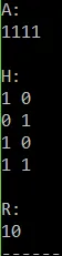
C-code:
#include <stdio.h>#define M 4#define N 2int main(){ int A[M] = {1,1,1,1}; int H[M][N] = {1,0,0,1,1,0,1,1}; int R[N]; int i, j; int res, temp; // print A printf("A:\n"); for(i = 0; i < M; i++){ printf("%d", A[i]); } printf("\n\n"); // print H printf("H:\n"); for(i = 0; i < M; i++){ for(j = 0; j < N; j++){ printf("%d ", H[i][j]); } printf("\n"); } printf("\n"); // calculate and print R printf("R:\n"); for(i = 0; i < N; i++){ res = 0; for(j = 0; j < M; j++){ temp = A[j] & H[j][i]; res = res ^ temp; } R[i] = res; printf("%d", R[i]); }}Running it gives us:
And we can clearly see that the way we will be storing H[M][N] in a memory will have a huge impact on the calculation process, cause the multiplication takes place on each column. A nice way is storing the matrix H column-by-column so that each step of the multiplication takes us to the next element of H with a simple counter.
Hardware architecture
The main diagram for our architecture looks like this:
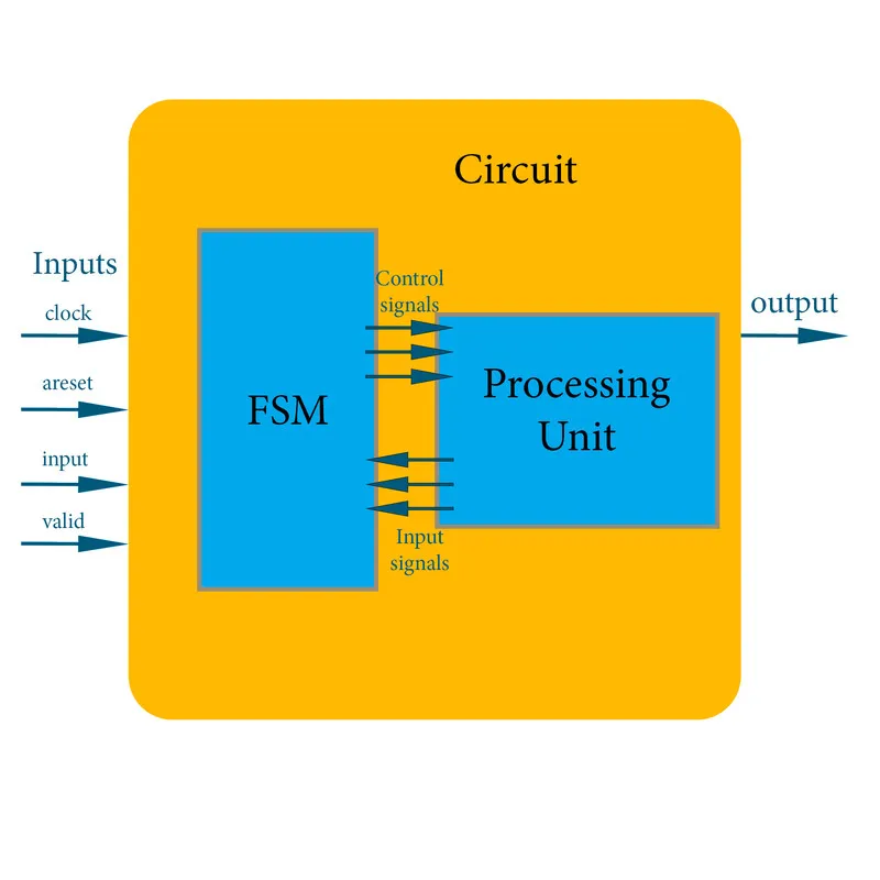
And so our circuit has 4 inputs, 1 output, a FSM and a processing unit which are:
- A clock input for the synchronous components (all actually)
- 1-bit asynchronous reset (areset) input that resets the system.
- 1-bit input to insert the bits for A.
- 1-bit valid input that tells the system if the given input is valid or not (for A[M]).
- 1-bit output to "extract" the bits of R.
- A control unit in the form of a FSM that manages the behavior of all the components.
- A processing unit that does the operation guided by the FSM.
Let's get into each one more in-depth...
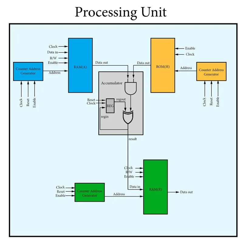
The Processing unit has:
- A ROM to store the H matrix, which means that it will be a constant "random" matrix (not an input to the system)
- Two separate RAM's to store the matrices A, R s so that we are able to write and read them.
- Counters for each memory component that also work as address generators.
- A accumulator that implements the XOR and AND operation in a single step.
You can see that the so called Accumulator (that we previously called "calculation unit") is a component that has a register (REG) that stores the "previous" result everytime. It does a AND operation between the A[i] and H[j][i] bits and XOR's this result with the previous result we had. When there is no previous result than the value will of course need to be 0 (zero) which can be done using the reset signal/input of the register and so accumulator.
Also note that we can also use only one counter (the one of ROMH) which has log(NM) bits that can be split into logN and logM for RAM(R) and RAM(A) respectively (I will maybe do it!) by keeping the "whole" counter for ROM(H).
Of course all these components are interconnected with wires/signals and the R/W, reset, enable signals are being controlled by the FSM which is:
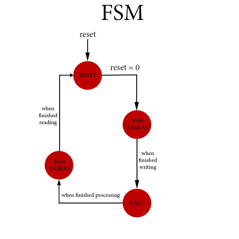
We have the states:
- RESET, which is the initial state where we go with an asynchronous reset signal to the main system. In this state all the components are being reseted (registers, counters, FSM).
- Write RAM(A), where we write the input bit into RAM(A) when having a "valid" input by the "user" by which can be seen by the valid bit input.
- CALC, which is the calculation state. Here we multiply the matrices A and H by reading from RAM(A) and ROM(H), calculate the result via the accumulator and finally also store the result into RAM(R).
- Read RAM(R), where we read the result calculated that has been stored in RAM(R).
The state transistions can be implemented very easily by using the values of the counters. At each state we of course have to "send out" the correct control signals to the components. In the first and last state the behavior is simple, but for the other two the control signals might even change inside of the state by checking the value of the valid bit (State 2) or even the value of some counter (State 3).
References:
- For the mathematical equations I used quicklatex!
- The diagrams are all made by myself
Previous posts of this series (should be here)
This section is so lonely, give it a hug!
And this is actually it for today's post guys and girls! I will see you next time again where we will start implementing the circuit in VHDL. I hope that you will enjoy this series!
Bye!